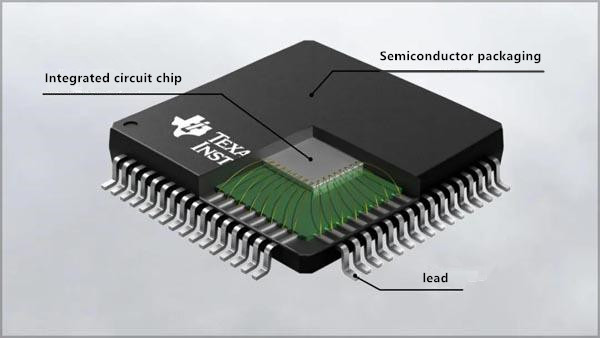
Description: The packaging workshop is mainly responsible for packaging core components such as chips and electronic components to protect them from the external environment, while ensuring product stability and reliability. The packaging process has a decisive impact on the performance and service life of electronic products, so the packaging shop occupies a pivotal position in the entire production chain.
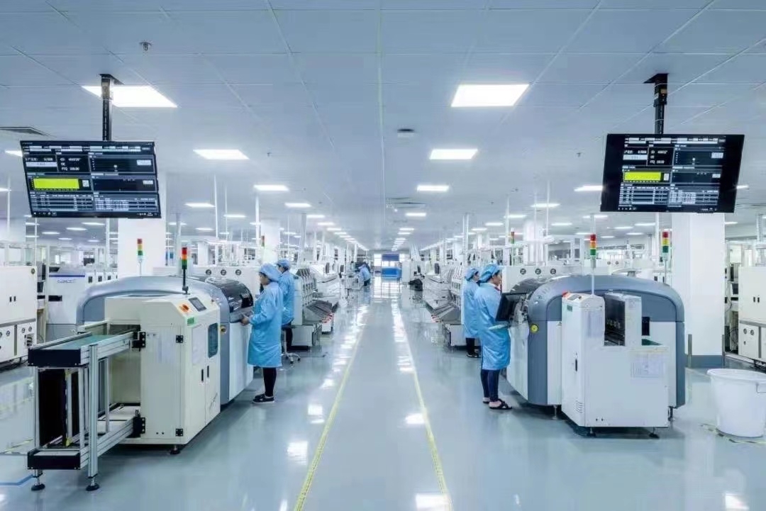
In 2025, the company plans to invest a new capital of 120 million yuan in Shenzhen. Sakata construction 6000m² modern standard clean workshop, complete 5 production lines, the use of domestic and foreign advanced packaging equipment: 72 sets. Such as: wafer grinding machine, wafer slicing machine, automatic loading machine, chip bonding machine, automatic plastic sealing system, cutting system and other related equipment. With advanced equipment and advanced technology not only improve the packaging efficiency of products, but also ensure the stability and consistency of packaged products. In addition, we continue to introduce new technologies and new equipment to meet the growing needs of the market.

Strict quality system: Quality is the lifeline of semiconductor packaging workshop. We have established a perfect quality control system, from the procurement of raw materials, production process control to the inspection of finished products, every link is strictly checked. Through continuous quality improvement and innovation, we ensure that every product that leaves the factory meets the highest international standards.

Environmental protection and sustainable development: In the semiconductor packaging workshop, we always adhere to the concept of environmental protection and sustainable development. Through the introduction of environmental protection equipment and technology, reduce energy consumption and emissions in the production process and reduce the impact on the environment. At the same time, we are also committed to recycling and waste treatment to achieve green production.
In the future, we will continue to increase scientific and technological innovation, improve the intelligent and automated level of semiconductor packaging workshop; We will pay close attention to the market dynamics, continue to expand business areas, to provide customers with better quality, more efficient packaging services, let us work together to create a better future, contribute to the progress of science and technology!
 Scan to add WeChat